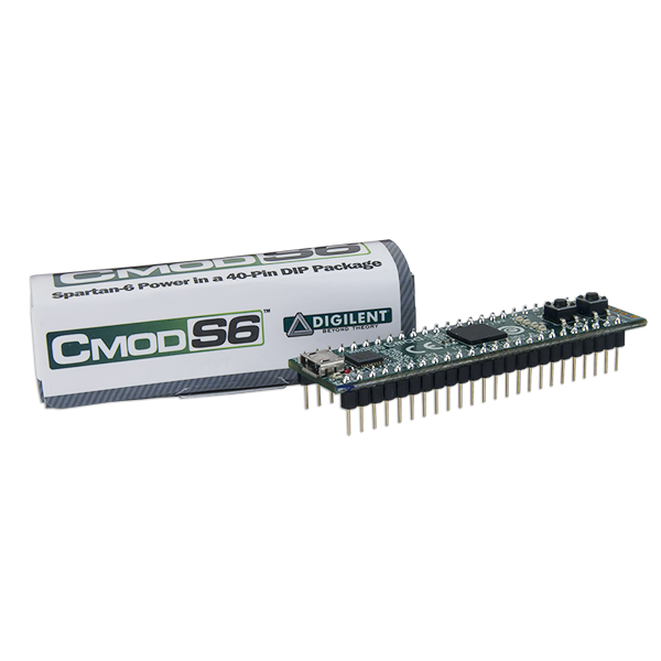
Cmod S6 Reference Manual
The Cmod S6 is retired and no longer for sale in our store.
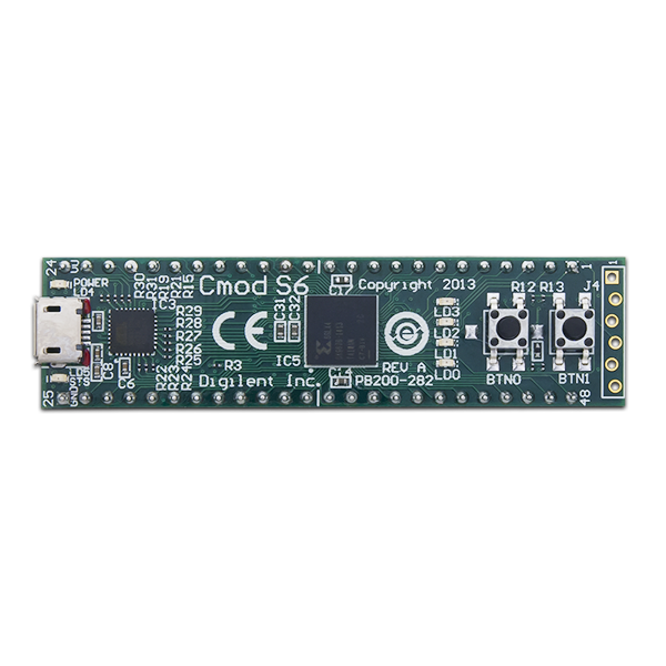
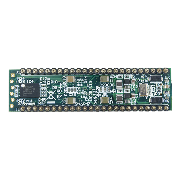
The Digilent Cmod S6 is a small, 48-pin DIP form factor board built around a Xilinx Spartan 6 LX4 FPGA. The board also includes a programming ROM, clock source, USB programming and data transfer circuit, power supplies, and basic I/O devices. There are 46 FPGA I/O signals that are routed to 100-mil-spaced through-hole pins, making the Cmod S6 well suited for use with solderless breadboards. At just .7” by 2.6” inches, it can also be loaded in a standard socket and used in embedded systems.


Download This Reference Manual
Features
- 600 slices (each with 4 LUTs and eight flip-flops)
- 8 DSP slices
- 216Kbits of block RAM
- 2 CMTs (4 DCMs and 2 PLLs)
- 16Mbyte Spansion Quad SPI Flash for storing FPGA configurations and/or user data
- 46 FPGA GPIO signals brought to DIP pins;
- Two on-board clock sources
- 4 user LEDs and 2 user buttons
- On-board Adept USB2 port for configuration, test and communications interfaces
1 Configuration
The FPGA on the Cmod S6 can be configured using the on-board Adept USB interface or from the on-board QuadSPI Flash memory. Configuration files can be programmed using Xilinx’s ISE 14.2 (or higher) development tools, using Digilent’s Adept system, or using older versions of the Xilinx tools if Adept is also installed.
Xilinx’s ISE/Impact programming tool and Digilent’s Adept tool will recognize the board and/or FPGA when the board is attached to a PC using a Type-A to micro-B USB cable. Xilinx’s iMPACT tool and Digilent’s Adept can both be used to program the FPGA, and iMPACT can also be used to program the on-board QSPI Flash. Please refer to the ISE and/or Adept documentation for more information on using the configuration software.
When using Digilent’s Adept software for programming, a dialog box available from the Config tab can be used to select a configuraiton file. Pressing the Program button will program the FPGA with the selected file. This may result in a warning that the configuration file was built for an unknown device; however, this warning can be ignored.
When using Xilinx’s iMPACT 14.2 (or higher) software for programming, a .bit file can be associated with the FPGA by right-clicking on the FPGA icon, selecting the desired .bit file, and clicking Program. On power-up, if the FPGA detects a valid bitstream stored in the Quad SPI flash memory, the FPGA will automatically configure itself with that bitstream. If necessary, the user can reconfigure the FPGA with a different bitstream at any point after power-up using iMPACT or Adept.
2 FPGA
The Cmod S6 features a Xilinx Spartan 6 XC6SLX4-2CPG196 FPGA. Of the 92 available unshared FPGA I/O pins, 46 are routed to through-hole pins on the DIP module, 24 are not connected, 14 are used by the programming interface, and 7 drive on-board I/Os (4 leds, 2 pushbuttons, and 2 clock inputs). Several of the 46 signals connected to FPGA pins are routed to clock buffers, and several are routed to matched pairs. Please see the schematic for more information.
The Spartan 6 LX4 FPGA includes 3,840 6-LUT logic cells, 4,800 flip-flops, 216Kb of block RAM, 8 DSP slices, and two clock management tiles, each with two DCMs and one PLL. The fabric can support internal clock speeds above 400MHz, allowing the Cmod S6 to host high-speed or complex designs. Please see the Spartan 6 user manual available at www.xilinx.com for more detailed information.
3 Power
The Cmod S6 can be powered either from a USB-connected computer, or from a power source connected to DIP pin 24 that delivers voltage in the range of 5VDC to 15VDC (the power input on pin 24 is most useful when the board is used in an embedded system or in a solderless breadboard). The two sources are diode-OR’ed on the board, so both may be connected simultaneously.
The FPGA and other on-board devices require 3.3VDC and 1.2VDC – both of these voltages are generated from the input supply using Texas Instrument’s TPS62170 switching regulators. Total current draw depends on FPGA configuration. When about half the FPGA is configured and running at 8MHz, the board consumes about 180mA from the main supply.
All user and dedicated I/O pins on the FPGA are rated for a maximum input voltage range of -0.60VDC to 4.10VDC. The recommended operating input voltage range for the pins is -0.5VDC to 4.0VDC with a maximum current rating of 10 mA when forward biasing the ground clamp diode. More detailed information about the usage and characteristics of the IO pins may be found at www.xilinx.com in documents UG381 and DS162.
4 Clocks
An 8MHz and a 1Hz clock are available to the FPGA. Both are generated from the on board USB processor, both are routed to clock inputs on the FPGA, and both run continuously. The 8MHz clock, called “FPGA-GCLK”, can be used with the FPGA’s clock manager to create a wide range of frequencies, even beyond 200MHz. The 1Hz clock provides a simple timing signal for basic experiments and low-frequency needs.
5 Quad SPI Flash Memory
The Cmod S6 includes a non-volatile 16Mbyte Spansion Quad SPI Flash that can store FPGA configuration files as well as user data. The Spansion device supports the standard 4-wire SPI protocol, as well as the newer Quad I/O and Dual I/O protocols at speeds from 50 MHz to 133 MHz, depending on the protocol and command used. For more information on the SPI Flash memory, please see the “S25FL128S and S25FL256S Data Sheet” at www.spansion.com.
To achieve the fastest programming speed over the Digilent USB-JTAG connection, when generating the bitstream in Project Navigator, change the SPI bus width to four and enable bitsream compression. To do this, simply select “Generate Programming File” and navigate to Process>Process Properties. In the pop-up menu, enable –g Compress under “Synthesis Options” and set –g SPI_buswidth to four under “Configuration Options”.
6 Digilent EPP Interface
The Cmod S6 implements the Digilent EPP interface (DEPP) for 8-bit parallel data transfers between the FPGA and a computer attached via the USB Micro connector. DEPP is based on a set of API’s available in the Adept 2 public SDK, available from the Adept product page at www.digilentinc.com. These APIs work in concert with firmware running on the USB controller to provide a high-level software interface for transporting data between a PC and the Cmod S6. To use the DEPP interface, the host PC must use software built from the Adept SDK DEPP libraries, and the FPGA has to be running a configuration that implements a DEPP controller. For a description of the DEPP library API, refer to the “DEPP Programmer's Reference Manual” included with the Adept 2 SDK. For information on designing a DEPP controller, refer to the “Digilent Asynchronous Parallel Interface (DEPP)” document, also included with the Adept 2 SDK.
7 Pin-out Diagram
This pin-out diagram shows the physical pin locations with the net names from the CmodS6 UCF file.


8 Factory Loaded User Demo
The Quad SPI Flash is loaded with a configuration file at the factory. When powered on, the file will configure the FPGA such that the buttons control the states of two LEDs, while the other two LEDs toggle at a speed of about 1 Hz. The general purpose I/O pins are initially configured as inputs, and are pulled up internally by the FPGA to read a logic level ‘1’. Each individual pin can be controlled using the DEPP interface to either drive the pin as an output, or to read the logic level that is present on the pin as an input.
The I/O pins can be controlled by writing to specific DEPP register addresses. To test the interface, the “Register I/O” tab within the Adept 2 application can be used. Table 1, shown below, gives a description of register addresses and functions.
| Address (HEX) | Function |
| 0 (0x0) | Stores the logic value present on pins 1 through 8 |
| 1 (0x1) | Stores the logic value present on pins 9 through 16 |
| 2 (0x2) | Stores the logic value present on pins 17 through 23 |
| 3 (0x3) | Stores the logic value present on pins 26 through 33 |
| 4 (0x4) | Stores the logic value present on pins 34 through 41 |
| 5 (0x5) | Stores the logic value present on pins 42 through 48 |
| 6 (0x6) | Controls the I/O state of pins 1 through 8 |
| 7 (0x7) | Controls the I/O state of pins 9 through 16 |
| 8 (0x8) | Controls the I/O state of pins 17 through 23 |
| 9 (0x9) | Controls the I/O state of pins 26 through 33 |
| 10 (0xA) | Controls the I/O state of pins 34 through 41 |
| 11 (0xB) | Controls the I/O state of pins 42 through 48 |
| Table 1. DEPP Register Map for factory loaded configuration. | |
The least significant bit in any register corresponds to the smallest pin number that it controls. Registers 6 through 11 will set up a pin controlled by registers 0 through 5 as an input if the corresponding bit in the register is a logic ‘1’ and will set up the pin as an output if the corresponding bit in the register is a logic ‘0’. For example, if the value stored in register 6 is 11110000 in binary (0xF0 in HEX), the pins 1-4 on the Cmod S6 will be set as outputs and pins 5-8 will be set as inputs. When a pin is configured as an output, it will initially be driven low (logic ‘0’).
The source code for this project can be found on the Cmod S6 product page of the Digilent website, www.digilentinc.com.